经典原版书库
点击查看第二章
点击查看第三章
计算机组成与体系结构:性能设计(英文版·原书第10版)
Computer Organization and Architecture: Designing for Performance,Tenth Edition
[美] 威廉·斯托林斯(William Stallings) 著
CHAPTER 1
Basic Concepts and Computer Evolution
Learning OBJectives
After studying this chapter, you should be able to:
- Explain the general functions and structure of a digital computer.
- Present an overview of the evolution of computer technology from early digital computers to the latest microprocessors.
- Present an overview of the evolution of the x86 architecture.
- Define embedded systems and list some of the requirements and constraints that various embedded systems must meet.
1.1 ORGANIZATION AND ARCHITECTURE
In describing computers, a distinction is often made between computer ardvtec- ture and computer organization. Although it is difficult to give precise definitions for these terms, a consensus exists about the general areas covered by each. For example, see [ VRAN80]. [SIEW82], and [BELL78a]: an interesting alternative view is presented in [REDD76].
Computer architecture refers to those attributes of a system visible to a programmer or. put another way, those attribulcs that have a direct impact on the logical execution of a program. A term lhai is often used interchangeably with computer architecture is instruction set architecture (ISA). The ISA defines instruction formats, instruction opcodes. registers, instruction and data memory; the effect of executed instructions on the registers and memory: and an algorithm for conlrol- ling instruction execution. Computer organization refers to the operational units and their interconnections that realize the architectural specifications. Exampks of architectural attributes include the instruction set. the number of bits used to represent various data types (e.g.. numbers, characters), I/O mechanisms, and techniques for addressing memory. Organizational attributes include those hardware details transparent to the programmer. such as control signals; interfaces between the computer and peripherals; and the memory technology used.
For example, it is an architectural design issue whether a computer will Eave a multiply instruction. It is an organizational issue whether that instruction will be implemented by a special multiply unit or by a mechanism that makes repeated use of the add unit of the system. "Die organizational decision may be based on the anticipated frequency of use of the multiply instruction, the relative speed of the two approaches, and the cost and physical size of a special multiply unit.
Historically, and still today, the distinction between archit eel urc and organization has been an important one. Many computer manufacturers offer a family of computer models, all with the same architecture but with differences in organization. Consequently, the different models in the family have different price and performance characteristics. Furthermore. a particular architcclurc may span many years and encompass a number of different computer models, its organization changing with changing technology. A prominent example of both these phenomena is the IBM Systcm/370 architecture. This architecture was first introduced in 1970 and indudcd a number of models. The customer with modest requirements could buy a cheaper. slower model and. if demand increased, later upgrade to a more expensive, faster model without having to abandon software that had already been developed. Over the years. IBM has introduced many new models with improved technology to replace older models, offering the customer greater speed, lower cost. or both. These newer models retained the same architecture so (ha( the customer's software investment was protected. Remarkably, the Systcm/370 architcclurc. with a few enhancements. has survived to this day as the architecture of IBM's mainframe product line.
In a class of computers called microcomputers, the relationship between architecture and organization is very close. Changes in technology not only influence organization but also result in the introduction of more powerful and more complex architectures. Generally, there is less of a requirement for gcncration-to-gcncration compatibility for these smaller machines. Thus, there is more interplay between organizational and architectural design decisions. An intriguing example of this is the reduced instruction set computer (RISC), which we examine in Chapter 15.
This book examines both computer organization and computer architecture. The emphasis is perhaps more on the side of organization. However, because a computer organization must be designed to implement a particular architectural specification, a thorough treatment of organization requires a detailed examination of architecture as well.
1.2 STRUCTURE AND FUNCTION
A computer is a complex system: contemporary computers contain millions of elementary electronic components. How. then, can one clearly describe them? The key is to recognize the hierarchical nature of most complex systems, including the computer [SIMO96]. A hierarchical system is a set of interrelated subsystems, each of the latter, in turn, hierarchical in structure until we reach some lowest level of elementary subsystem.
The hierarchical nature of complex systems is essential to both their design and their description. The designer need only deal with a particular level of the system at a time. At each level the system consists of a set of components and their interrelationships. The behavior at each level depends only on a simplified, abstracted characterization of the system at the next lower level. At each level, the designer is concerned with structure and function:
- Structure: The way in which the components arc interrelated.
- Function: The operation of each individual component as part of the structure.
In terms of description, we have two choices: starting at the bottom and building up to a complete description, or beginning with a top view and decomposing the system into its subparts. Evidence from a number of fields suggests that the top- down approach is the clearest and most effective [WEIN75].
The approach (aken in this book follows from this viewpoint. The computer system will be described from the top down. We begin with the major components of a computer. describing their structure and function, and proceed to successively lower layers of the hierarchy. The remainder of this section provides a very brief overview of this plan of attack.
Function
Both the structure and functioning of a computer arc. in essence, simple. In general terms, there arc only four basic functions that a computer can perform:
- Data processing: Data may take a wide variety of forms, and the range of processing requirements is broad. However. we shall see that there arc only a few fundamental methods or types of data processing.
- Data storage: Even if the computer is processing data on the fly (i.c.. data come in and get processed, and the results go out immediately), the computer must temporarily store at least those pieces of data (ha( arc being worked on at any given moment. Thus, there is at least a short-term data storage function. Equally important. the computer performs a long-term data storage function. Files of data arc stored on the computer for subsequent retrieval and update.
- Data movement: The computer's operating environment consists of devices (ha( serve as either sources or destinations of data. When data are received from or delivered to a device that is directly connected to the computer. the process is known as input-output (HO), and the device is referred to as a peripheral. When data arc moved over longer distances, to or from a remote device, the process is known as data communications.
- Control: Within I he computer. a control unit manages the computer's resources and orchestrates the performance of its functional parts in response to instructions.
The preceding discussion may seem absurdly generalized. It is certainly possible. even at a top level of computer structure, to differentiate a variety of functions. but to quote [SIEW82]:
There is remarkably little shaping of computer structure to fit the function to be performed. At the root of this lies the general-purpose nature of computers. in which all the functional specialization occurs at the time of programming and not at the time of design.
Structure
We now look in a general way at the internal structure of a computer. We begin with a (raditionai computer with a single processor that employs a microprogrammed control unit, then examine a typical multicorc structure.
SIMPLE SINGLE-PROCESSOR COXfPUTER Figure 1.1 provides a hierarchical view of the internal structure of a traditional single-processor computer. There arc four main structural components:
- Central processing unit (CPU): Controls the operation of the computer and performs its data processing functions; often simply referred to as processor.
- Main memory: Stores data.

- I/O: Moves data between the computer and its external environment.
- System interconnection: Some mechanism that provides for communication among CPU. main memory, and I/O. A common example of system interconnection is by means of a system bus. consisting of a number of conducting wires to which all the other components attach.
There may be one or more of cadi of the aforementioned components. Traditionally. there has been just a single processor. In recent years, there has been increasing use of multiple processors in a single computer. Some design issues relating to multiple processors crop up and arc discussed as the text proceeds; Part Five focuses on such computers.
Each of these components will be examined in some detail in Part Two. However. for our purposes, the most interesting and in some ways the most complex component is the CPU. Its major structural components arc as follows:
- Control unit: Controls the operation of the CPU and hence the computer.
- Arithmetic and logic unit (ALU): Performs the computer's data processing functions.
- Registers: Provides storage internal to the CPU.
- CPU interconnection: Some mechanism (ha( provides for communication among the control unit, ALU, and registers.
Part Three covers these components, where we will see that complexity is added by the use of parallel and pipelined organizational techniques. Finally, there arc several approaches to the implementation of the control unit; one common approach is a microprogrammed implement al ion. In essence. a microprogrammed control unit operates by executing microinstructions that define the functionality of the control unit. With this approach. the structure of the control unit can be depicted, as in Figure 1.1. This structure is examined in Part Four.
MULTICORE COMPUTER STRUCTURE As was mentioned, contemporary computers generally have multiple processors. When these processors ail reside on a single chip, the term multicore computer is used, and each processing unit (consisting of a control unit. ALU. registers, and perhaps cache) is called a core. To clanly the terminology, this text will use the following definitions.
- Central processing unit (CPU): That portion of a computer that fetches and executes instructions. It consists of an ALU. a control unit. and registers. In a system with a single processing unit, it is often simply referred to as a processor.
- Core: An individual processing unit on a processor chip. A core may be cquiv- aicnl in functionality to a CPU on a single-CPU system. Other specialized processing units. such as one optimized for vector and matrix operations, arc also referred to as cores.
- Processor: A physical piece of silicon containing one or more cores. The processor is the computer component that interprets and executes instructions. If a processor contains multiple cores, i( is referred to as a multicore processor.
After about a decade of discussion, there is broad industry consensus on this usage. Another prominent feature of contemporary computers is the use of multiple layers of memory. called cache memory, between the processor and main memory. Chapter 4 is devoted to the topic of cache memory. For our purposes in this section, we simply note that a cache memory is smaller and faster than main memory ar.d is used to speed up memory access, by placing in the cache data from main memory, (hat is likely to be used in the near future. A greater performance improvement may be obtained by using multiple levels of cache, with level 1 (LI) closest to the core and additional levels (L2. L3, and so on) progressively farther from the core. In this scheme. level n is smaller and faster (han level n + 1.
Figure 12 is a simplified view of the principal components of a typical mul- ticorc computer. Most computers, including embedded computers in smartphones and tablets. plus personal computers, laptops, and workstations, arc housed on a motherboard. Before describing this arrangement. we need to define some terms. A printed circuit board (PCB) is a rigid, flat board (ha( holds and interconnects chips and other electronic components. The board is made of layers. typically two to ten. that interconnect components via copper pathways that arc etched into the board. The main printed circuit board in a computer is called a system board or motherboard, while smaller ones that plug into the slots in the main board arc called expansion boards.
The most prominent elements on the motherboard arc the chips. A chip is a single piece of semiconducting material, typically silicon, upon which electronic circuits and logic gates arc fabricated. The resulting product is referred to as an integrated circuit.
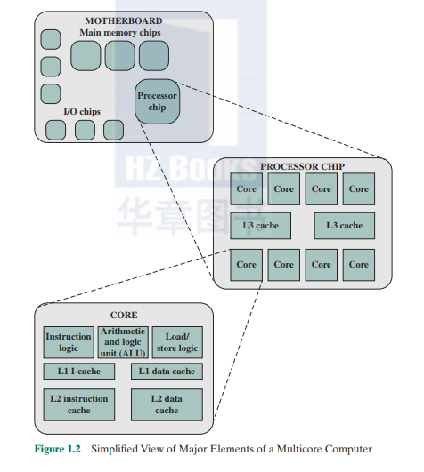
Figure 12 Simplified View of Major Elements of a Multicore Computer
The motherboard contains a slot or socket for the processor chip, which typically contains multiple individual cores, in what is known as a nudticoreprocessor. There arc also slots for memory chips. I/O controller chips, and other key computer components. For desktop computers, expansion slots enable the inclusion of more components on expansion boards. Thus, a modem motherboard connects only a few individual chip components, with each chip containing from a few thousand up to hundreds of millions of transistors.
Figure 12 shows a processor chip that contains eight cores and an L3 cache. Not shown is the logic required to control operations between the cores and the cache and between the cores and the external circuitry on the motherboard. The figure indicates that the L3 cache occupies two distinct portions of the chip surface. However. typically. ail cores have access to the entire L3 cache via the aforementioned control circuits. The processor chip shown in Figure 1.2 docs not represent any specific product. but provides a general idea of how such chips arc laid out.
Next. we zoom in on the structure of a single core. which occupies a portion of the processor chip. In general terms, the functional elements of a core arc:
- Instruction logic: This includes the tasks involved in fetching instructions, and decoding each instruction to determine the instruction operation and the memory locations of any operands.
- Arithmetic and logic unit (ALU): Performs the operation specified by an instruction.
- Load/storc logic: Manages the transfer of data to and from main memory via cache.
The core also contains an LI cache, split between an instruction cache (I-cachc) that is used for the transfer of instructions to and from main memory. and an LI data cache. for the transfer of operands and results. Typically, today's processor chips also include an L2 cache as part of the core. In many eases, this cache is also split between instruction and data caches, although a combined, singk L2 cache is also used.
Keep in mind that this representation of the layout of the core is only intended to give a general idea of internal core structure. In a given product, the functional elements may not be laid out as the three distinct elements shown in Figure 1.2, especially if some or ail of these functions arc implemented as part of a microprogrammed control unit.
EXAMPLES 1( will be instructive to look at some real-world examples that illustrate the hierarchical structure of computers. Figure 13 is a photograph of the motherboard for a computer built around two Intel Ouad-Corc Xcon processor chips. Many of the elements labeled on the photograph arc discussed subsequently in this book. Here. we mention the most important. in addition to the processor sockets:
- PCI-Express slots for a high-end display adapter and for additional peripherals (Section 3.6 describes PCIc).
- Ethernet controller and Ethernet ports for network connections.
- USB sockets for peripheral devices.
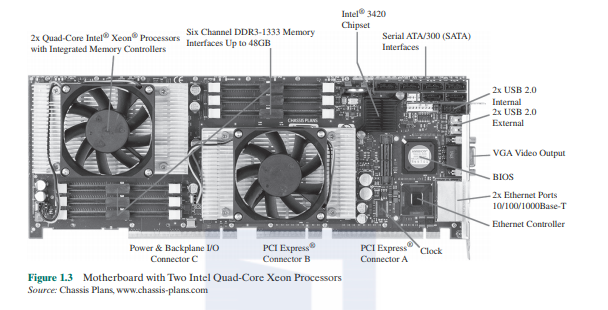
- Serial ATA (SATA) sockets for connection to disk memory (Section 7.7 discusses Ethernet, USB. and SATA).
- Interfaces for DDR (double data rate) main memory chips (Section 53 discusses DDR).
- Intel 3420 chipset is an I/O controller for direct memory access operations between peripheral devices and main memory (Section 7.5 discusses DDR).
Following our top-down strategy, as illustrated in Figures 1.1 and 1.2, wc can now zoom in and look at the internal slructurc of a processor chip. For variety, wc look at an IBM chip instead of the Intel processor chip. Figure 1.4 is a photograph of the processor chip for the IBM zEntcrprise EC12 mainframe computer. This chip has 2.75 billion transistors. The superimposed labels indicate how the silicon real estate of the chip is allocated. Wc sec that this chip has six cores. or processors. In addition, there arc two large areas labeled L3 cache, which arc shared by all six processors. The L3 control logic controls traffic between the L3 cache and the cores and between the L3 cache and the external environment. Additionally, there is storage control (SC) logic between the cores and the L3 cache. The memory controller (MC) function controls access to memory external to the chip. The GX I/O bus controls the interface to the channel adapters accessing the I/O.
Going down one level deeper. wc examine the internal structure of a single core. as shown in the photograph of Figure 15. Keep in mind that this is a portion of the silicon surface area making up a single-processor chip. The main sub-areas within this core area arc the following:
- ISU (instruction sequence unit): Determines the sequence in which instructions arc executed in what is referivd to as a superscalar architecture (Chapter 16).
- IFU (instruction fetdi unit): Logic for fetching instructions.
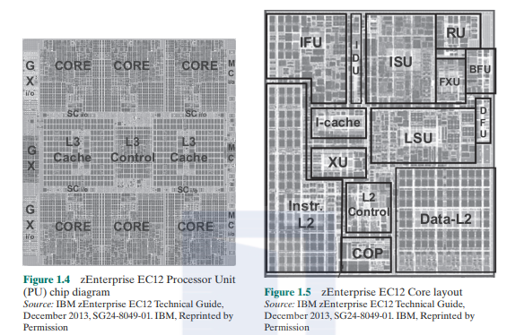
- IDU (instruction decode unit): The IDU is fed from the IFU buffers, and is responsible for the parsing and decoding of all z/Archilecture operation codes.
- LSU (load-store unit): The LSU contains the 96-kB LI data cache.1 and manages data traffic between the L2 data cache and the functional execution units. It is responsible for handling ail types of operand accesses of all lengths, modes. and formats as defined in the z/Archilecture.
- XU (translation unit): This unit translates logical addresses from instructions into physical addresses in main memory. The XU also contains a translation lookaside buffer (TLB) used to speed up memory access. TLBs arc discussed in Chapter 8.
- FXU (fixed-puint unit): Hie FXU executes fixed-point arithmetic operations.
- BFU (binary floating-point unit): The BFU handles ail binary and hexadecimal floating-point operations, asweii as fixed-point multiplication operations.
- DFU (decimal floating-point unit): The DFU handles both fixed-point and floating-point operations on numbers that arc stored as decimal digits.
- RD (recover) unit): The RU keeps a copy of the complete state of the system that includes ail registers, collects hardware fault signals, and manages the hardware recovery actions.
- COP (dedicated co-processor): The COP is responsible for data compression and encryption functions for each core.
- I-cache: This is a 64-kB LI instruction cache. allowing the IFU to prefetch instructions before they arc needed.
- L2 control: This is the control logic that manages the traffic through the two L2 caches.
- Data-L2: A 1-MB L2 data cache for all memory traffic other than instructions.
- Instr-L2: A 1-MB L2 instruction cache.
As we progress through the book, the concepts introduced in this section will become clearer.
1.3 A BRIEF HISTORY OF COMPUTERS
In this section, we provide a brief overview of the history of the development of computers. This history is interesting in itself, but more importantly, provides a basic introduction to many important concepts that we deal with throughout the book.
The First Generation: Vacuum Tubes
The first generation of computers used vacuum tubes for digital logic elements and memory. A number of research and lhen commercial computers were built using vacuum tubes. For our purposes, it will be instructive to examine perhaps the most famous first-gvneration computer. known as the IAS computer.
A fundamental design approach first implemented in the IAS computer is known as the stored-progratn concept. This idea is usually attributed to the mathematician John von Neumann. Alan Turing developed the idea at about the same time. The first publication of the idea was in a 1945 proposal by von Neumann for a new computer. the EDVAC (Electronic Discrete Variable Computer).
In 1946, von Neumann and his colleagues began the design of a new stored- program computer. referred to as the IAS computer. at the Princeton Institute for Advanced Studies. The IAS computer. although not completed until 1952. is the prototype of ail subsequent general-purpose computers.
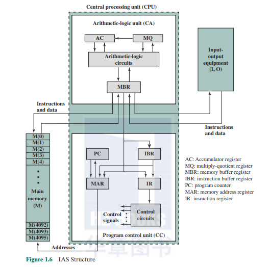
Figure 1.6 shows the structure of the IAS computer (compare with Figure 1.1). It consists of
- A main memory, which stores both data and instructions'
-
An arithmetic and logic unit (ALU) capable of operating on binary data
- A control unit, which interprets the instructions in memory and causes them to be executed
- Input-output (I/O) equipment operated by the control unit
This structure was outlined in von Neumann's earlier proposal, which is worth quoting in part at this point [VONN45]:
- 2.2 First: Since the device is primarily a computer. it will have to perform the elementary operations of arithmetic most frequently. These arc addition, subtraction, multiplication, and division. It is therefore reasonable that it should contain specialized organs for just these operations.
It must be observed, however. that while this principle as such is probably sound, the specific way in which it is realized requires close scrutiny. At any rate a central arithmetical part of the device will probably have to exist, and this constitutes the first specific part: CA.
2.3 Second: The logical control of the device. that is. the proper sequencing of its operations, can be most efficiently carried out by a central control organ. If the device is to be elastic, that is. as nearly as possible all purpose, then a distinction must be made between the specific instructions given for and defining a particular problem, and the general control organs that see to it that these instructions—no matter what they arc—arc carried out. The former must be stored in some way; the latter arc represented by definite operating parts of the device. By the central control we mean this latter function only. and the organs that perform it form the second specific part: CC.
2.4 Third: Any device that is to carry out long and complicated sequences of operations (specifically of calculations) must have a considerable memory
The instructions which govern a complicated problem may constitute considerable material, particularly so if the code is circumstantial (which it is in most arrangements). This material must be remembered.
At any rate, the total memory constitutes the third specific part of the device: M.
2.6The three specific parts CA. CC (together C), and M correspond to the associative neurons in the human nervous system. It remains to discuss the equivalents of the sensory or afferent and the motor or efferent neurons. These arc the input and output organs of the device.
The device must be endowed with the ability to maintain input and output (sensory and motor) contact with some specific medium of this type. The medium will be called the outside recording medium of the device: R.
2.7Fourth: The device must have organs to transfer information from R into its specific parts C and M. These organs form its input, the fourth specific part: I. It will be seen that it is best to make ail transfers from R (by I) into M and never directly from C.
2.8Fifth: The device must have organs to transfer from its specific parts C and M into R. These organs form its output, the fifth specific part: O. It will be seen that it is again best to make all transfers from M (by O) into R. and never directly from C.
With rare exceptions, ail of today's computers have this same general structure and function and arc thus referred to as von Neumann machines. Thus, it is worthwhile at this point to describe briefly the operation of the IAS computer [BURK46, GOLD54]. Following [HAYE98]. the terminology and notation of von Neumann arc changed in the foilouing to conform more closely to modem usage; the examples accompanying this discussion arc based on that latter text.
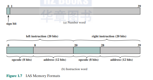
The memory of the IAS consists of 4.096 storage locations, called worth, of 40 binary digits (bits) each.Both data and instructions arc stored there. Numbers arc represented in binary form, and each instruction is a binary code. Figure 1.7 illustrates these formats. Each number is represented by a sign bit and a 39-bit value. A word may alternatively contain two 2()-bit instructions, wilh each instruction consisting of an 8-bit operation code (opcode) specifying the operation to be performed and a 12-bit address designating one of the words in memory (numbered from 0 to 999).
The control unit operates the IAS by fetching instructions from mcirory and executing them one at a time. We explain these operations with reference to Figure 1.6. This figure reveals that both the control unit and the ALU contain storage locations, called registers, defined as follows:
- Memory buffer register (MBR): Contains a word to be stoiud in memory orient to the I/O unit.or is used to receive a word from memory or from the I/O unit.
- Memory address register (MAR): Specifies the address in memory of the word to be written from or read into the MBR.
- Instruction register (IR): Contains the 8-bit opcode instruction being executed.
- Instruction buffer register (IBR): Employed to hold temporarily the righthand instruction from a word in memory.
- Program counter (PC): Contains the address of the next instruction pair to be fetched from memory.
- Accumulator (AC) and multiplier quotient (MQ): Employed to hold temporarily operands and results of ALU operations. For example. the result of multiplying two 4()-bit numbers is an 8()-bit number; the most significant 40 bits are stored in the AC and the least significant in the MQ.
The IAS operates by repetitively performing an instruction cycle, as sho^n in Figure 1.8. Each instruction cyde consists of two subcycles. During the fetch cycle, the opcode of the next instruction is loaded into the IR and the address portion is loaded into the MAR. This instruclion may be taken from the IBR, or it can be obtained from memory by loading a word into the MBR. and then down to the 1BR. IR. and MAR.
Why the indirection? These operations are controlled by electronic circuitry and result in the use of data paths. To simplify the electronics, there is only one register that is used lo specify the address in memory for a read or wrile and only one register used for the source or destination.

Once the opcode is in the IR. the execute cyde is performed. Control circuitry interprets the opcode and executes the instruction by sending out the appropriate control signals to cause data to be moved or an operation to be performed by the ALU.
The IAS computer had a total of 21 instructions, which arc listed in Table 1.1. These can be grouped as follows:
- Data transfer: Move data between memory and ALU registers or between two ALU registers.
- Unconditional hranch: Normally. the control unit executes instructions in sequence from memory. This sequence can be changed by a branch instruction. which facilitates repetitive operations.
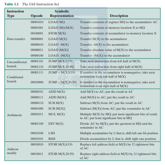
- Conditional branch: The branch can be made dependent on a condition, thus allowing decision points.
- Arithmetic: Operations performed by the ALU.
- Address modify: Permits addresses to be computed in the ALU and then inserted into instructions stored in memory. This allows a program considerable addressing flexibility.
Table 1.1 presents instructions (excluding I/O instructions) in a symbolic, easy-to-rcad form. In binary form, each instruction must conform to the format of Figure 1.7b. The opcode portion (first 8 bits) specifics which of the 21 instructions is to be executed. The address portion (remaining 12 bits) specifics which of the 4.096 memory locations is to be involved in the execution of the instruction.
Figure 1.8 shows several examples of instruction execution by the control unit. Note that each operation requires several steps, some of which arc quite elaborate. The multiplication operation requires 39 subopcralions. one for each bit position except that of the sign bit.
The Second Generation: Transistors
The first major change in the electronic computer came with the replacement of the vacuum tube by the transistor. The transistor, which is smaller. cheaper, and generates less heat than a vacuum tube, can be used in the same way as a vacuum tube to construct computers. Unlike the vacuum tube, which requires wiivs. metal plates, a glass capsule, and a vacuum, the transistor is a solid-stale device, made from silicon.
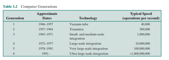
The transistor was invented at Beil Labs in 1947 and by the 1950s had launched an electronic revolution. It was not until the late 1950s, however, that fully transistorized computers were commercially available. The use of the transistor defines the second generation of computers. It has become widely accepted to classify computers into generations based on the fundamental hardware technology employed (Table 1.2). Each new generation is characterized by greater processing performance. larger memory capacity. and smaller size than the previous one.
But there arc other changes as well. The second generation saw the introduction of more complex arithmetic and logic units and control units, the use of high-level programming languages, and the provision of system software with the
- In broad terms, system software provided the ability to load programs, move data to peripherak. and libraries to perform common computations, similar to what modem operating systems, such as Windows and Linux, do.
It will be useful to examine an important member of the second generation: the IBM 7094 [BELL71]. From the introduction of the 7(X) series in 1952 to the introduction of the last member of the 7000 series in 1964. this IBM product line underwent an evolution that is typical of computer products. Successive members of the product line showed increased performance, increased capacity, and/or lower cost.
The size of main memory. in multiples of 210 36-bit words, grew from 2k (lk= 210) to 32k words,' while the time to access one word of memory, the memory cycle time, fell from 30 μs to 1.4 μs. "Die number of opcodes grew from a modest 24 to 185.
Also. over the lifetime of this series of computers, the relative speed of the CPU increased by a factor of 50. Speed improvements arc achieved by improved electronics (e.g.. a transistor implementation is faster than a vacuum tube implementation) and more complex circuitry. For example, the IBM 7094 includes an Instruction Backup Register. used to buffer the next instruction. The control unit fetches two adjacent words from memory for an instruction fetch. Except for the occurrence of a branching instruction, which is relatively infrequent (perhaps 10 to 15%), this means that the control unit has to access memory for an instruction on only half the instruction cycles. This prefetching significantly reduces the average instruction cycle time.
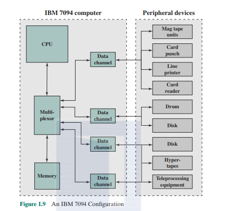
Figure 1.9 shows a large (many peripherals) configuration for an IBM 7)94, which is representative of second-generation computers. Several differences from the IAS computer arc worth noting. The most important of these is the use of data channels. A data channel is an independent I/O module with its own processor and instruction set. In a computer system with such devices, the CPU docs not execute dclaiicd I/O instructions. Such instructions arc stored in a main memory to be executed by a special-purpose processor in the data channel itself. The CPU initiates an I/O transfer by sending a control signa! to the data channel, instructing it to execute a sequence of instructions in memory. The data channel performs its task independently of the CPU and signals the CPU when the operation is complete. This arrangement relieves the CPU of a considerable processing burden.
Another new feature is the multiplexor, which is the central termination point for data channels, the CPU. and memory. The multiplexor schedules access to the memory from the CPU and data channels. allowing these devices to act independently.
The Third Generation: Integrated Circuits
A single, self-contained transistor is called a discrete component. Throughout the 1950s and early 1960s, electronic equipment was composed largely of discrete components—transistors, resistors, capacitors, and so on. Discrete components were manufactured separately, packaged in their own containers, and soldered or wired together onto Masonitc-likc circuit boards, which were then installed in computers, oscilloscopes.and other electronic equipment. Whenever an electronic device called for a transistor, a little tube of metal containing a pinhead-sized piece of silicon had to be soklcred to a circuit board.The entire manufacturing process, from transistor to circuit board, was expensive and cumbersome.
These facts of life were beginning to create problems in the computer industry. Early second-generation computers contained about 1O.(XX) transistors. This figure grew to the hundreds of thousands, making the manufacture of newer. more powerful machines increasingly difficult.
In 1958 came the achievement that revolutionized electronics and started the era of microelectronics: the invention of the integrated circuit. It is the integrated circuit that defines the third generation of computers. In this section, we provide a brief introduction to the technology of integrated circuits. Then we look at perhaps the two most important members of the third generation, both of which were introduced at the beginning of that era: the IBM Systcm/360 and the DEC PDP-8.
MICROELECTRONICS Microelectronics means, literally, "small electronics." Since the beginnings of digital electronics and the computer industry, there has been a persistent and consistent trend toward the reduction in size of digital electronic circuits. Before examining the implications and benefits of this trend, we need to say something about the nature of digital electronics. A more detailed discussion is found in Chapter 11.
The basic elements of a digital computer. as wc know, must perform data storage. movement, processing, and control functions. Only two fundamental types of components arc required (Figure 1.10): gates and memory cells. A gate is a device (ha( implements a simple Boolean or logical function. For example. an AND gate with inputs A and B and output C implements the expression IF A AND B ARE TRUE THEN C IS TRUE. Such devices arc called gates because they control data flow in much the same way (hat canal gates control the flow of water. The memory cell is a device (ha( can store 1 bit of data; (hat is. the device can be in one of two stable states at any time. By interconnecting large numbers of these fundamental devices, wc can construct a computer. Wc can relate this to our four basic functions as follows:
- Data storage: Provided by memory cells.
- Data processing: Provided by gates.
- Data movement: The paths among components arc used to move data from memory to memory and from memory through gates to memory.
- Control: The paths among components can carry control signals. For example, a gate will have one or two data inputs plus a control signal input that activates the gate. When the control signal is ON. the gate performs its function on the data inputs and produces a data output. Conversely, when the control signal is OFF. the output line is null, such as the one produced by a high impedance state. Similarly, the memory cell will store the bit that is on its input lead when the WKl l t control signal is ON and will place the bi( that is in the cell on its output lead when the READ control signal is ON.
Thus, a computer consists of gates, memory cells, and interconnections among these elements. The gates and memory cells are. in turn, constructed of simple electronic components, such as transistors and capacitors.
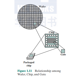
The integrated circuit exploits the fact that such components as transistors, resistors, and conductors can be fabricated from a semiconductor such as silicon. It is merely an extension of the solid-state art to fabricate an entire circuit in a tiny piece of silicon rather than assemble discrete components made from separate pieces of silicon into the same circuit. Many transistors can be produced at the same time on a single wafer of silicon. Equally important, these transistors can be connected with a process of metallization to form circuits.
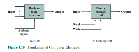
Figure 1.11 depicts the key concepts in an integrated circuit. A thin wafer of silicon is divided into a matrix of small areas, each a few millimeters square. The identical circuit pattern is fabricated in each area. and the wafer is broken up into chips. Each chip consists of many gates and/or memory cells plus a number of input and output attachment points. This chip is then packaged in housing that protects it and provides pins for attachment to devices beyond the chip. A number of these packages can then be interconnected on a printed circuit board to produce larger and more complex circuits.
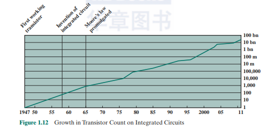
Initially. only a few gates or memory ccDs could be reliably manufactured and packaged together. These early integrated circuits arc referred to as small-scale integration (SSI). As time went on. it became possible to pack more and more components on the same chip. This growth in density is illustrated in Figure 1.12; i( is one of the most remarkable technological trends ever recorded.8 This figure refbets the famous Moore's law. which was propounded by Gordon Moore, cofound er of Intel, in 1965 [MOOR65]. Moore observed that the number of transistors that could be put on a single chip was doubling every year. and correctly predicted that (his pace would continue into the near future. To the surprise of many, including Moore, the pace continued year after year and decade after decade. The pace slowed to a doubling every 18 months in the 1970s but has sustained that rate ever since.
The consequences of Moore's law arc profound:
- The cost of a chip has remained virtually unchanged during this period of rapid growth in density. This means that the cost of computer logic and memory circuitry has fallen at a dramatic rate.
- Because logic and memory elements arc placed closer together on irorc densely packed chips, the electrical path length is shortened, increasing operating speed.
- The computer becomes smaller, making it more convenient to place in a variety of environments.
- There is a reduction in power requirements.
- The interconnections on the integrated circuit arc much more reliable than solder connections. With more circuitry on each chip, there arc fewer inter chip connections.
IBM SYSTEM/360 By 1964. IBM had a firm grip on the computer market *ith its 7000 series of machines. In that year. IBM announced the Systcm/360. a new family of computer products. Although the announcement itself was no surprise, it contained some unpleasant news for current IBM customers: the 360 product line was incompatible with okicr IBM machines. Thus, the transition to the 360 would be difficult for the current customer base, but IBM felt this was necessary to break out of some of the constraints of the 7000 architecture and to produce a system capable of evolving with the new integrated circuit technology [PADE81. GIFF87]. The strategy paid off both financially and technically. The 360 was the success of the decade and cemented IBM as the overwhelmingly dominant computer vendor, with a market share above 70%. And. with some modifications and extensions, the architecture of the 360 remains to this day the architecture of IBM's mainframe computers. Examples using this architecture can be found throughout this text.
The Systcm/360 was the industry's first planned family of computers. The family covered a wide range of performance and cost. The models were compatible in the sense that a program written for one model should be capable of being executed by another model in the series, with only a difference in the time it lakes to execute.
The concept of a family of compatible compute is was both novel and extremely successful. A customer with modest requirements and a budget to match could start with the relatively inexpensive Model 30. Later, if the customer's needs grew, it was possible to upgrade to a faster machine with more memory without sacrificing the investment in already-developed software. The characteristics of a family arc as follows:
- Similar or identical instruction set In many eases, the exact same set of machine instructions is supported on ail members of the family. Thus, a program that executes on one machine will also execute on any other. In some cases, the lower end of the family has an instruction set that is a subset of that of the top end of the family.This means that programs can move up but not down.
- Similar or identical operating system: The same basic operating system is available for ail family members. In some cases, additional features arc added to the higher-end members.
- Increasing speed: The rate of instruction execution increases in going from lower to higher family members.
- Increasing number of I/O ports: The number of I/O ports increases in going from lower to higher family members.
- Increasing memory size: The size of main memory increases in going from lower to higher family members.
- Increasing cost: At a given point in time, the cost of a system increases in going from lower to higher family members.
How could such a family concept be implemented? Differences were achieved based on three factors: basic speed, size, and degree of simultaneity [STEV64]. For example. greater speed in the execution of a given instruction coukl be gained by the use of more complex circuitry in the ALU, allowing subopcrations to be carried out in parallel. Another way of increasing speed was to increase the width of the data path between main memory and the CPU. On the Model 30. only 1 byte (8 bits) coukl be fetched from main memory at a time. whereas 8 bytes coukl be fetched at a time on the Model 75.
The Systcm/360 not only dictated the future course of IBM but also had a profound impact on the entire industry. Many of its features have become standard on other large computers.
DEC PDP-8 In the same year that IBM shipped its first Systcm/360. another momentous first shipment occurred: PDP-8 from Digital Equipment Corporation (DEC). At a time when the average computer required an air-conditioned room, the PDP-8 (dubbed a minicomputer by the industry. after the miniskirt of the day) was small enough that it could be placed on top of a lab bench or be built into other equipment. It could not do everything the mainframe could, but at $16000. it was cheap enough for each lab technician to have one. In contrast. the Syslcm/360 series of mainframe computers introduced just a few months before cost hundreds of thousands of dollars.
The low cost and small size of the PDP-8 enabled another manufacturer to purchase a PDP-8 and integrate i( into a total system for resale. These other manufacturers came to be known as original equipment manufacturers (OEMs), and the OEM market became and remains a major segment of the computer marketplace.
In contrast to the central-switched architecture (Figure 1.9) used by IBM on its 700/7000 and 360 systems, later models of the PDP-8 used a structure that became virtually universal for microcomputers: the bus structure. This is illustrated in Figure 1.13. The PDP-8 bus. called the Omnibus, consists of 96 separate signal paths, used to carry control, address, and data signals. Because ail system components share a common set of signal paths, their use can be controlled by the CPU. This architecture is highly flexible, allowing modules to be plugged into the bus to create various configurations. It is only in recent years that the bus structure has given way to a structure known as point-to-point interconnect, described in Chapter 3.
Later Generations
Beyond the third generation there is less general agreement on de (ini ng gc nc rat ions of computers.Table 12 suggests that there have been a number of later generations, based on advances in integrated circuit technology. With the introduction of large- scale integration (LSI), more than 1.000 components can be placed on a single integrated circuit chip. Vcry-largc-scalc integration (VLSI) achieved more than 10.000 components per chip, while current ultra-large-scale integration (ULSI) chips can contain more than one billion components.
With the rapid pace of technology. the high rate of introduction of new products. and the importance of software and communications as well as hardware, the classification by generation becomes less clear and less meaningful. In this section, we mention two of the most important of developments in later generations.
SEMICONDUCTOR MEMORY The first application of integrated circuit technology to computers was the construction of the processor (the control unit and the arithmetic and logic unit) out of integrated circuit chips. But it was also found that this same technology could be used to construct memories.
In the 1950s and 1960s. most computer memory was constructed from tiny rings of ferromagnetic material, each about a sixteenth of an inch in diameter. These rings were strung up on grids of fine wires suspended on small screens inside the computer. Magnetized one way. a ring (called a core) represented a one; magnetized the other way, it stood for a zero. Magnetic-core memory was rather fast; it took as little as a millionth of a second to read a bit stored in memory. But it was

expensive and bulky. and used destructive readout: The simple act of reading a core erased the data stored in it. It was therefore necessary to install circuits to restore the data as soon as it had been extracted.
Then, in 1970. Fairchild produced the first relatively capacious semiconductor memory. This chip, about the size of a single core. could hold 256 bits of mcmoiy. It was nondestructive and much faster than core. It took only 70 billionths of a second to read a bit. However. the cost per bit was higher than for that of core.
In 1974. a seminal event occurred: The price per bit of semiconductor memory dropped below the price per bit of core memory. Following this, there has been a continuing and rapid dedinc in memory cost accompanied by a corresponding increase in physical memory density. This has led the way to smaller. faster machines with memory sizes of larger and more expensive machines from just a few years earlier. Developments in memory technology. together with developments in processor technology to be discussed next, changed the nature of computers in less than a decade. Although bulky, expensive computers remain a part of the landscape, the computer has also been brought out to the “end user." with office machines and personal computers.
Since 1970. semiconductor memory has been through 13 generations: Ik. 4k. 16k. 64k, 256k. IM, 4M, 16M. 64M. 256M. 1G. 4G, and. as of this writing. 8 Gb on a single chip (1 k = 2^10.1M = 2^20,1G = 2^30). Each generation has provided increased storage density, accompanied by declining cost per bit and declining access time. Densities arc projected to reach 16 Gb by 2018 and 32 Gb by 2023 [ITRS14].
MICROPROCESSORS Just as the density of elements on memory chips has continued to rise, so has the density of elements on processor chips. As time went on. more and more elements were placed on each chip. so that fewer and fewer chips were needed to construct a single computer processor.
A breakthrough was achieved in 1971. when Intel developed its 4004. The 4004 was the first chip to contain all of the components of a CPU on a single chip: The microprocessor was bom.
The 4004 can add two 4-bit numbers and can multiply only by repeated addition. By today's standards, the 4(XM is hopelessly primitive, but it marked the beginning of a continuing evolution of microprocessor capability and power.
This evolution can be seen most easily in the number of bits that the processor deals with at a time. There is no clear-cut measure of this, but perhaps the best measure is the data bus width: the number of bits of data that can be brought into or sent out of the processor at a time. Another measure is the number of bits in the accumulator or in the set of general-purpose registers. Often, these measures coincide, but not always. For example, a number of microprocessors were developed that operate on 16-bit numbers in registers but can only read and write 8 bits at a time.
The next major step in the evolution of the microprocessor was the introduction in 1972 of the Intel 8(X)8. This was the first 8-bit microprocessor and was almost twice as complex as the 4(X)4.
Neither of these steps was to have the impact of the next major event: the introduction in 1974 of the Intel 8080. This was the first general-purpose microprocessor. Whereas the 4(X)4 and the 8008 had been designed for specific applications, the 8080 was designed to be the CPU of a general-purpose microcomputer. Like the 8008. the 8080 is an 8-bil microprocessor. The 8080, however, is faster, has a richer instruction set, and has a large addressing capability.
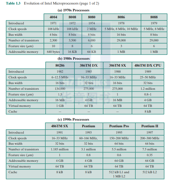
About the same time, 16-bit microprocessors began to be developed. However, it was not until the end of the 1970s that powerful, general-purpose 16-bit microprocessors appeared. One of these was the 8086. The next step in this trend occurred in 1981. when both Bell Labs and Hewlelt-Packard developed 32-bit, single-chip microprocessors. Intel introduced its own 32-bit microprocessor, the 80386Jn 1985 (Table 1.3).
1.4 THE EVOLUTION OF THE INTEL x86 ARCHITECTURE
Throughout this book, wc rely on many concrete examples of computer design and implementation to illustrate concepts and to illuminate trade-offs. Numerous systems. both contemporary and historical. provide examples of important computer architecture design features. But the book relies principally on examples from two processor families: the Intel x86 and the ARM architectures. 'Die current x86 offerings represent the results of decades of design effort on complex instruction set computers (CISCs).Thc x86 incorporates the sophisticated design principles once found only on mainframes and supercomputers and serves as an excellent example of CISC design. An alternative approach to processor design is the reduced instruction set computer (RISC). 'Die ARM architecturc is used in a wide variety of embedded systems and is one of the most powerful and best-designed RISC-based systems on the market. In this section and the next, wc provide a brief overview of these two systems.
In terms of market share. Intel has ranked as the number one maker of microprocessors for non-embedded systems for decades. a position i( seems unlikely to yield. 'Die evolution of its flagship microprocessor product serves as a good indicator of the evolution of computer technology in general.
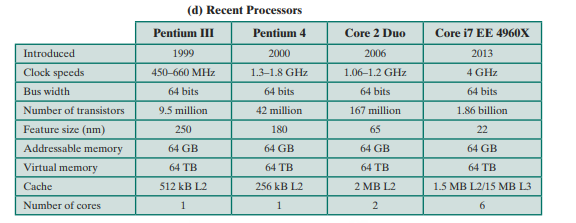
Table 1.3 shows that evolution. Interestingly, as microprocessors have grown faster and much more complex. Intel has actually picked up the pace. Intel used to develop microprocessors one after another. every four years. But Intel hopes to keep rivals at bay by trimming a year or two off this development time. and has done so with the most recent x86 generations.
It is worthwhile to list some of the highlights of the evolution of the Intel product line:
- 8080: The world's first general-purpose microprocessor. This was an £-bil machine. with an 8-bit data path to memory. The 8080 was used in the first personal computer, the Altair.
- 8086: A far more powerful. 16-bit machine. In addition to a wider data path and larger registers. the 8086 sported an instruction cache, or queue. that prefetches a few instructions before they arc executed. A variant of this processor. the 8088. was used in IBM's first personal computer. securing the success of Intel. The 8086 is the first appearance of the x86 architecture.
- 80286: This extension of the 8086 enabled addressing a 16-MB memory instead of just 1 MB.
- 80386: Intel's first 32-bit machine, and a major overhaul of the product. With a 32-bit architecture. the 80386 rivaled the complexity and power of minicomputers and mainframes introduced just a few years earlier. Ibis was the first Intel processor to support multitasking, meaning it could run multiple programs at the same time.
- 80486: The 80486 introduced the use of much more sophisticated and powerful cache technology and sophisticated instruelion pipelining. The 80486 also offered a built-in math coprocessor, offloading complex math operations from the main CPU.
- Pentium: With the Pentium. Intel introduced the use of superscalar techniques. which allow multiple instructions to execute in parallel.
- Pentium Pro: The Pentium Pro continued the move into superscalar organization begun with the Pentium, with aggressive use of register renaming, branch prediction, data flow analysis, and speculative execution.
- Pentium II: The Pentium II incorporated Intel MMX technology, which is designed specifically to process video. audio, and graphics data efficiently.
- Pentium III: The Pentium HI incorporates additional floating-point instructions: The Streaming SIMD Extensions (SSE) instruction set extension added 70 new instructions designed to increase performance when exactly the same operations arc to be performed on multiple data objects. Typical applications arc digital signal processing and graphics processing.
- Pentium 4: The Pentium 4 includes additional floating-point and other enhancements for multimedia.
- Core This is the first Intel x86 microprocessor with a dual core. referring to the implementation of two cores on a single chip.
- Core 2: The Core 2 extends the Core architecture to 64 bits. The Core 2 Quad provides four cores on a single chip. More recent Core offerings have up to 10 cores per chip. An important addition to the architecture was the Advanced Vector Extensions instruction set that provided a set of 256-bit. and then 512- bit. instructions for efficient processing of vector data.
Almost 40 years after its introduction in 1978. the x86 architecture continues to dominate the processor market outside of embedded systems. Although the organization and technology of the x86 machines have changed dramatically over the decades, the instruction set architecture has evolved to remain backward compatible with earlier versions. Thus, any program written on an oklcr version of the x86 architecture can execute on newer versions. All changes to the instruction set architecture have involved additions to the instruction set. with no subtractions. The rate of change has been the addition of roughly one instruction per month added to the architecture [ANTH08], so that there arc now thousands of instructions in the instruction set.
The x86 provides an excellent illustration of the advances in computer hardware over the past 35 years. The 1978 8086 was introduced with a clock speed of 5 MHz and had 29000 transistors. A six-core Core i7 EE 4960X introduced in 2013 operates at 4 GHz. a speedup of a factor of 800, and has 1.86 billion transistors, about 64000 times as many as the 8086. Yet the Core i7 EE 4960X is in only a slightly larger package than the 8086 and has a comparable cost.
1.5 EMBEDDED SYSTEMS
The term embedded system refers to the use of electronics and software within a product, as opposed to a general-purpose computer, such as a laptop or desk top system. Millions of computers arc sold every year. including laptops, personal computers. workstations, servers, mainframes, and supercomputers. In contrast, billions of computer systems arc produced each year that arc embedded within larger devices. Today. many, perhaps most.devices that use electric power have an embedded computing system. It is likely that in the near future virtually all such devices will have embedded computing systems.
Types of devices with embedded systems arc almost too numerous to list. Examples include cell phones. digital cameras, video cameras. calculators, microwave ovens, home security systems, washing machines. lighting systems, thermostats. printers, various automotive systems (e.g.. transmission control, cruise control, fuel injection. anti-lock brakes, and suspension systems), tennis rackets, toothbrushes, and numerous types of sensors and actuators in automated systems.
Often, embedded systems arc tightly coupled to their environment. This can give rise to real-time constraints imposed by the need to interact with the environment. Constraints, such as required speeds of motion, required precision of measurement. and required time durations, dictate the timing of software operations. If multiple activities must be managed simultaneously, this imposes more complex real-time constraints.
Figure 1.14 shows in general terms an embedded system organization. In addition to the processor and memory. there arc a number of elements (ha( differ from the typical desktop or laptop computer:
- There may be a variety of interfaces that enable the system to measure. manipulate. and otherwise interact with the external environment. Embedded systems often interact (sense, manipulate. and communicate) with external world through sensors and actuators and hence arc typically reactive systerrs; a reactive system is in continual interaction with the environment and executes at a pace determined by that environment.
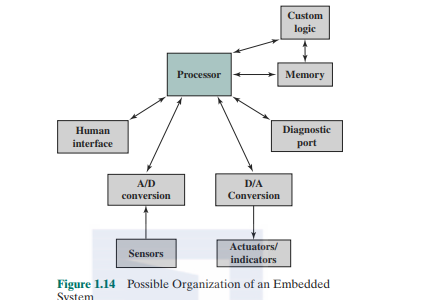
- The human interface may be as simple as a flashing light or as complicated as real-time robotic vision. In many cases, there is no human interface.
- The diagnostic port may be used for diagnosing the system (hat is being controlled—not just for diagnosing the computer.
- Special-purpose field programmable (FPGA). application-specific (ASIC), or even nondigitai hardware may be used to increase performance or reliability.
- Software often has a fixed function and is specific to the application.
- Efficiency is of paramount importance for embedded systems. They arc optimized for energy, code size, execution time, weight and dimensions, and cost.
There arc several noteworthy areas of similarity to gvncral-purposc computer systems as well:
- Even with nominally fixed function software, the ability to tick! upgrade to fix bugs, to improve security. and to add functionality, has become very important for embedded systems, and not just in consumer devices.
- One comparatively recent development has been of embedded system platforms that support a wide variety of apps. Good examples of this arc sir artphones and audio/visual devices, such as smart TVs.
The Internet of Things
It is worthwhile to separately callout one of the major drivers in the proliferation of embedded systems.'Die Internet of things (loT) is a term that refers to the expanding intcrconneclion of smart devices, ranging from appliances to tiny sensors. A dominant theme is the embedding of short-range mobile transceivers into a wide array of gadgets and everyday items, enabling new forms of communication between people and things, and between things themselves.Hie Internet now supports the interconnection of billions of industrial and personal objects, usually through cloud systems. The objects deliver sensor information.act on their environment, and. in some eases, modify themselves, to create overall management of a larger system, like a factory or city.
The loT is primarily driven by deeply embedded devices (defined below). These devices arc low-bandwidth, low-repetition data-caplure. and low-bandwidth data-usagc appliances that communicate with each other and provide data via user interfaces. Embedded appliances, such as high-resolution video security cameras, video VoIP phones. and a handful of others. require high-bandwidth streaming capabilities. Yet countless products simply require packets of data to be intermittently delivered.
With reference to the end systems supported, the Internet has gone through roughly four generations of deployment culminating in the loT:
- Inf ormation technology (IT): PCs. servers, routers, firewalls, and so on. bought as IT devices by enterprise IT people and primarily using wired connectivity.
- Operational technology (OT): Machincs/applianccs with embedded IT built by non-IT companies, such as medical machinery. SCADA (supervisory control and data acqusition), process control, and kiosks, bought appliancrs hy enterprise OT people and primarily using wired connectivity.
- Personal technology: Smartphones, tablets, and eBook readers bought as IT devices by consumers (employees) exclusively using wireless connectivity and often multiple forms of wireless connectivity.
- Sensor/actuator technology: Single-purpose devices bought by consumers. IT. and OT people exclusively using wireless connectivity, generally of a single form, as part of larger systems.
It is the fourth gcncraiion that is usually thought of as the loT. and it is marked by the use of billions of embedded devices.
Embedded Operating Systems
There are two general approaches to developing an embedded operating system (OS). 'Die first approach is to lake an existing OS and adapt i( for the embedded application. For example, there arc embedded versions of Linux. Windows, and Mac, as well as other commercial and proprietary operating systems specialized for embedded systems. Hie other approach is to design and implement an OS intended solely for embedded use. An example of the latter isTinyOS. widely used in wireless sensor networks. This topic is explored in depth in [STAL15].
Application Processors versus Dedicated Processors
In (his subsection, and the next two, we briefly introduce some terms commonly found in the literature on embedded systems. Application processors arc defined by the processor's ability to execute complex operating systems, such as Linux, Android, and Chrome.Thus, the application processor is gvncral-purposc in nalurc. A good example of the use of an embedded application processor is the smartphone. The embedded system is designed to support numerous apps and perform a wide variety of functions.
Most embedded systems employ a dedicated processor, which. as the name implies, is dedicated to one or a small number of specific tasks required by the host device. Because such an embedded system is dedicated to a specific task or tasks, the processor and associated components can be engineered to reduce size and cost.
Microprocessors versus Microcontrollers
As we have seen, early microprocessor chips included registers, an ALU, and some sort of control unit or instruction processing logic As transistor density incrcascd.it became possible to increase the complexity of the instruction set arch it eel tire, and ultimately to add memory and more than one processor. Contemporary microprocessor chips, as shown in Rgurc 12. include multiple cores and a substantial amount of cache memory.
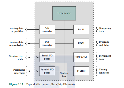
A microcontroller chip makes a substantially different use of the logic space available. Figure 1.15 shows in general terms the elements typically found on a microcontroller chip. As shown, a microcontroller is a single chip that contains the processor. non-volatile memory for the program (ROM). volatile memory for input and output (RAM), a clock, and an I/O control unit. "Die processor portion of the microcontroller has a much lower silicon area than other microprocessors and rruch higher energy efficiency. We examine microcontroller organization in more detail in Section 1.6.
Also called a "computer on a chip." billions of microcontroller units arc embedded each year in myriad products from toys to appliances to automobiles. For example. a single vehicle can use 70 or more microcon (rollers. Typically, especially for the smaller, less expensive microcontrollers, they arc used as dedicated processors for specific tasks. For example. microcontrollers arc heavily utilized in automation processes. By providing simple reactions to input. they can control machinery, turn fans on and off. open and close valves, and so forth. They arc integral parts of modem industrial technology and arc among the most inexpensive ways to produce machinery that can handle extremely complex functionalities.
Microcontrollers come in a range of physical sizes and processing power. Processors range from 4-bit to 32-bit architectures. Microcontrollers tend to be rruch slower than microprocessors, typically operating in the MHz range rather than the GHz speeds of microprocessors. Another typical feature of a microcontroller is that it docs not provide for human interaction. The microcontroller is programmed for a specific task, embedded in its device, and executes as and when required.
Embedded versus Deeply Embedded Systems
We have. in this section, defined the concept of an embedded system. A subset of embedded systems, and a quite numerous subset. is referred to as deeply embedded systems. Although this term is widely used in the technical and commercial
literature, you will search the Internet in vain (or at least I did) for a straighlfor- ward definition. Generally, we can say that a deeply embedded system has a processor whose behavior is difficult to observe both by the programmer and the user. A deeply embedded system uses a microcontroller rather than a microprocessor. is not programmable once the program logic for the device has been burned into ROM (read-only memory), and has no interaction with a user.
Deeply embedded systems arc dedicated, single-purpose devices that detect something in the environment, perform a basic level of processing, and then do something with the results. Deeply embedded systems often have wireless capability and appear in networked configurations, such as networks of sensors deployed over a large area (e.g.. factory, agricultural fickl).Thc Internet of things depends heavily on deeply embedded systems. Typically, deeply embedded systems have extreme resource constraints in terms of memory, processor size, time, and power consumption.
1.6 ARM ARCHITECTURE
The ARM architecture refers to a processor architecture that has evolved from RISC design principles and is used in embedded systems. Chapter 15 examines RISC design principles in detail. In this section, we give a brief overview of the ARM ardiitccturc.
ARM Evolution
ARM is a family of RISC-based microprocessors and microcontrollers designed by ARM Holdings. Cambridge. England. Hie company doesn't make processors but instead designs microprocessor and multicorc architectures and licenses them to manufacturers. Specifically. A RM Holdings has two types of licensable products: processors and processor architectures. For processors, the customer buys the rights to use ARM-supplied design in their own chips. For a processor architecture, the customer buys the rights to design their own processor compliant with ARM's architecture.
ARM chips arc high-speed processors that arc known for their small die size and low power requirements. They arc widely used in smartphones and other handheld devices, including game systems, as well as a large variety of consumer products. ARM chips arc the processors in Apple's popular iPod and iPhone devices, and arc used in virtually all Android smartphones as well. ARM is probably the most widely used embedded processor architecture and indeed the most widely used processor architecture of any kind in the world [VANCI4].
The origins of ARM technology can be traced back to the British-based Acorn Computers company. In the early 1980s. Acorn was awarded a contract by the British Broadcasting Corporation (BBC) to develop a new microcomputer architecture for the BBC Computer Literacy Project. The success of this contract enabled Acorn to go on to develop the first commercial RISC processor, the Acorn RISC Machine (ARM). The first version. ARM1. became operational in 1985 and was used for internal research and development as well as being used as a coprocessor in the BBC machine.
In this early stage. Acorn used the company VLSI Technology to do the actual fabrication of the processor chips. VLSI was licensed to market the chip on its own and had some success in getting other companies to use the ARM in their products, particularly as an embedded processor.
The ARM design matched a growing commercial need for a high-performance, low-powcr-consumption. small-size, and low-cosi processor for embedded applications. But further development was beyond the scope of Acorn's capabilities. Accordingly, a new company was organized, with Acorn. VLSI. and Apple Computer as founding partners, known as ARM Ltd. The Acorn RISC Machine became Advanced RISC Machines.
Instruction Set Architecture
The ARM instruction set is highly regular. designed for eflident implementation of the processor and efficient execution. AU instructions arc 32 bits long and follow a regular format. This makes the ARM ISA suitable for implementation over a wide range of products.
Augmenting the basic ARM ISA is the Thumb instruction set. which is a rc- encodcd subset of the ARM instruction set. Thumb is designed to increase the performance of ARM implementations that use a 16-bit or narrower memory data bus.
”The company dropped the designation Advanced RISC Machines in the late 1990s. It is now simply known as the ARM architecture. and to allow belter code density than provided by the ARM instruction set. The Thumb instruction set contains a subset of the ARM 32-bit instruction set recoded into 16-bit instructions. "Die current defined version is Thumb-2.
The ARM and Thumb-2 ISAs arc discussed in Chapters 12 and 13.
ARM Products
ARM Holdings licenses a number of specialized microprocessors and related technologies. but the bulk of their product line is the Cortex family of microprocessor architectures. There arc three Cortex architectures, conveniently labeled wilh the initials A. R. and M.
COR TEX-A/CORTEX-A 50 The Cortex-A and Cortex-A50 arc application processors, intended for mobile devices such as smartphones and eBook readers, as well as consumer devices such as digital TV and home gateways (e.g.. DSL and cable Internet modems). These processors run at higher clock frequency (over 1 GHz), and support a memory management unit (MMU). which is required for full feature OSs such as Linux. Android. MS Windows, and mobile OSs. An MMU is a hardware module that supports virtual memory and paging by (ranslating virtual addresses into physical addresses; this topic is explored in Chapter 8.
The two architectures use both the ARM and Thumb-2 instruction sets; the principal difference is that the Cortex-A is a 32-bit machine. and the Cortcx-A50 is a 64-bit machine.
CORTEX-R The Cortex-R is designed to support real-time applications, in which the timing of events needs to be controlled with rapid response to events. They can run at a fairly high clock frequency (e.g., 200MHz to 800MHz) and have very low response latcn^. The Cortex-R includes enhancements both to the instruction set and to the processor organization to support deeply embedded real-time devices. Most of these processors do not have MMU: the limited data requirements and the limited number of simultaneous processes eliminates the need for elaborate hardware and software support for virtual memory. The Cortex-R docs have a Memory Protection Unit (MPU), cache, and other memory features designed for industrial applications. An MPU is a hardware module that prohibits one program in memory from accidentally accessing memory assigned to another active program. Using various methods, a protective boundary is created around the program, and instructions within the program arc prohibited from referencing data outside of that boundary.
Examples of embedded systems that would use the Corlcx-R arc automotive braking systems, mass storage controllers, and networking and printing devices.
CORTEX-M Cortex-M series processors have been developed primarily for the microcontroller domain where the need for fast, highly deterministic intenupt management is coupled with the desire for extremely low gate count and lowest possible power consumption. As with the Cortex-R series, the Cortex-M architecture has an MPU but no MMU. The Cortex-M uses only the Thumb-2 instruction set. The market for the Cortex-M includes loT devices. wireless scnsor/actuator networks used in factories and other enterprises, automotive body electronics, and so on.
There arc currently four versions of the Cortex-M series:
- Cortex-M0: Designed for 8- and 16-bit applications, this model emphasizes low cost, ultra low power, and simplicity. It is optimized for small silicon die size (starting from 12k gates) and use in the lowest cost chips.
- Cortex-M0+: An enhanced version of the MO that is more energy efficient.
- Cortex-M3: Designed for 16- and 32-bit applications, this model emphasizes performance and energy efficiency. It also has comprehensive debug and trace features to enable software developers to develop their applications quickly.
- Cortex-M4: This model provides all the features of the Corlcx-M3, with additional instructions to support digital signal processing tasks.
In this text, we will primarily use the ARM Cortcx-M3 as our example embedded system processor. It is the best suited of all ARM models for general-purpose microcontroller use. The Cortex-M3 is used by a variety of manufacturers of microcontroller products. Initial microcontroller devices from lead partners already combine the Cortcx-M3 processor with flash. SRAM, and multiple peripherals to provide a competitive offering at the price of just $1.
Figure 1.16 provides a block diagram of the EFM32 microcontroller from Silicon Labs. The figure also shows detail of the Cortex-M3 processor and core components. We examine each level in turn.
The Cortex-M3 core makes use of separate buses for instructions and data. Thk arrangement k smeHmes referretl tn as » Harvard architcctiin'!, in contract with the von Neumann architecture, which uses the same signal buses and memory for both instructions and data. By being able to read both an instruction and data from memory at the same time, the Cortcx-M3 processor can perform rrany operations in parallel, speeding application execution. The core contains a decoder for Thumb instructions, an advanced ALU wth support for hardware multiply and divide. control logic. and interfaces to the other components of the processor. In particular. there is an interface to the neslcd vector interrupt controller (N VIC) and the embedded trace macroccll (ETM) module.
The core is part of a module called the Cortex-M3 processor. This term is somewhat misleading, because typically in the literature, the terms core and processor arc viewed as equivalent. In addition to the core. the processor includes the following elements:
- NVIC: Provides configurable interrupt handling abilities to the processor. It facilitates low-latcn(^ exception and interrupt handling. and controls power management.
- ETM: An optional debug component that enables reconstruction of program execution. The ETM is designed to be a high-speed. low-power debug tool (ha( only supports instruction trace.
- Debug access port (DAP): This provides an interface for external debug access to the processor.
-
Debug logic: Basic debug functionality includes processor halt, single-step, processor core register access.
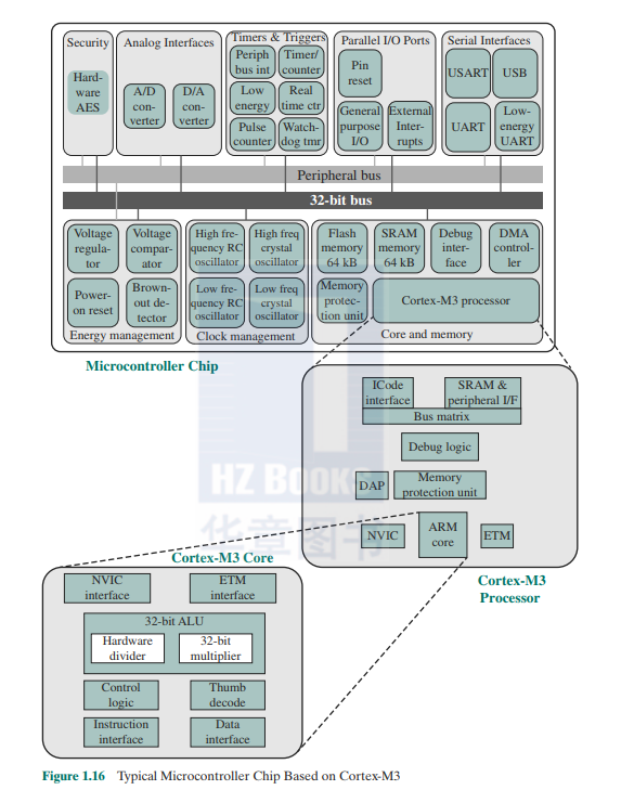
- ICode interface: Fetches instructions from the code memory space.
- SRAM & peripheral interface: Rcad/writc interface to data memory and peripheral devices.
- Bus matrix: Connects the core and debug interfaces to external buses on the microcontroller.
- Memory protection unit: Protects critical data used by the operating system from user applications, separating processing tasks by disallowing access to each other's data, disabling access to memory regions, allowing memory regions to be defined as read-only, and detecting unexpected memory accesses (hat coukl potentially break the system.
The upper part of Figure 1.16 shows the block diagram of a typical microcontroller built with the Cortcx-M3. in this ease the EFM32 microcontroller. This microcontroller is marketed for use in a wide variety of devices, including energy, gas, and water metering; alarm and security systems: industrial automation devices; home automation devices; smart accessories: and health and fitness devices. The silicon chip consists of 10 main areas:1'
- Core and memory: This region includes the Cortex-M3 processor. static RAM (SRAM) data memory.14 and flash memory1' for storing program instructions and nonvarying application data. Flash memory is nonvolatile (data is not lost when power is shut off) and so is ideal for this purpose. The SRAM stores variable data This area akn include a debug interface, which it tn reprogram and update the system in the field.
- Parallel I/O ports: Configurable for a variety of parallel I/O schemes.
- Serial interfaces: Supports various serial I/O schemes.
- Analog interfaces Analog-to-digital and digital-to-analog logic to support sensors and actuators.
- Timers and triggers: Keeps track of timing and counts events, generates output waveforms, and triggers timed actions in other peripherals.
- Clock management: Controls the clocks and oscillators on the chip. Multiple clocks and oscillators arc used to minimize power consumption and provide short startup times.
- Energy management: Manages the various low-energy modes of operation of the processor and peripherals to provide real-time management of the energy needs so as to minimize energy consumption.
-
Security: The chip includes a hardware implementation of the Advanced Encryption Standard (AES).
32-bit bus: Connects ail of the components on the chip. - Peripheral bus: A network which lets the different peripheral module communicate directly with each other without involving the processor. This supports timing-critical operation and reduces software overhead.
Comparing Figure 1.16 with Figure 12. you will see many similarities and the same general hierarchical structure. Note, however. that the top level of a microcontroller computer system is a single chip. whereas for a multicorc computer. the top level is a motherboard containing a number of chips. Another noteworthy difference is that there is no cache, neither in the Cortcx-M3 processor nor in the microcontroller as a whole. which plays an important role if the code or data resides in external memory. Though the number of cycles to read the instruction or data varies depending on cache hit or miss, the cache greatly improves the performance when external memory is used. Such overhead is not needed for a microcontroller.
1.7 CLOUD COMPUTING
Although the general concepts for cloud computing go back to the 1950s. ebud computing services first became available in the early 2000s. particularly targeted at large enterprises. Since then, doud computing has spread to small and medium size businesses, and must recently to consumers. Apple's iCloud was launched in 2012 and had 20 million users within a week of launch. Eve mote, the cloud-based notetaking and archiving service, launched in 2008. approached 100 million users in less than 6 years. In this section, we provide a brief overview. Cloud computing is examined in more detail in Chapter 17
Basic Concepts
There is an increasingly prominent trend in many organizations to move a substantial portion or even all information technology (IT) operations to an Intemet-connected infrastructure known as enterprise cloud computing. At the same time. individual users of PCs and mobile devices arc relying more and more on cloud computing services to backup data, synch devices, and share, using personal cloud computing. NIST defines cloud computing, in NIST SP-800-145 (The NIST Definition of Cloud Computing), as follows:
Cloud computing: A model for enabling ubiquitous, convenient, on-demand network access to a shared pool of configurable computing resources (eg., networks, servers, storage, applications, and services) that can be rapidly provisioned and released with minimal management effort or service provider interaction.
Basically, with cloud computing, you get economies of scale. professional network management, and professional security management. These featurescan be attractive to companies large and small, government agencies, and individual PC and mobile users. The individual or company only needs to pay for the storage capacity and services they need. The user, be it company or individual, doesn't Eave the hassle of setting up a database system, acquiring the hardware they need, doing maintenance, and backing up the data—all these arc part of the cloud service.
In theory. another big advantage of using cloud computing to store your data and share it with others is that the cloud provider takes care of security. Alas, the customer is not always protected. There have been a number of security failures among cloud providers. Eve mote made headlines in early 2013 when it told ail of its users to reset their passwords after an intrusion was discovered.
Cloud networking refers to the networks and network management functionality that must be in place to enable cloud computing. Most cloud computing solutions rely on the Internet. but that is only a piece of the networking infrastructure. One example of cloud networking is the provisioning of high-performance and/or high-reliability networking between the provider and subscriber. In this ease. some or ail of the traffic between an enterprise and the doud bypasses the Internet and uses dedicated private network facilities owned or leased by the doud service provider. More generally, cloud networking refers to the collection of network capabilities required to access a cloud, including making use of specialized services over the Internet, linking enterprise data centers to a cloud, and using firewalls and other network security devices al critical points to enforce access security policies.
We can think of cloud storage as a subset of cloud computing. In essence, ebud storage consists of database storage and database applications hosted remotely on cloud servers. Cloud storage enables small businesses and individual users to take advantage of data storage that scales with their needs and to take advantage of a variety of database applications without having to buy. maintain, and manage the storage assets.
Cloud Services
The essential purpose of cloud computing is to provide for the convenient rental of computing resources. A cloud service provider (CSP) maintains computing and data storage resources that arc available over the Internet or private networks. Customers can rent a portion of these resources as needed. Virtually all cloud service is provided using one of three modek (Figure 1.17): SaaS. PaaS, and laaS.which we examine in this section.
SOFTWARE AS A SERVICE (SAAS) As the name implies, a SaaS cloud provides service to customers in the form of software. specifically application software, running on and accessible in the cloud. SaaS follows the familiar model of Web services, in this ease applied to cloud resources. SaaS enables the customer to use the cloud provider's applications running on the provider's cloud infrastructure. The applications arc accessible from various dient devices through a simple interface such as a Web browser. Instead of obtaining desktop and server licenses for software products it uses, an enterprise obtains the same functions from the ebud service. SaaS saves the complexity of software installation, maintenance, upgrades, and patches. Examples of services at (his level arc Gmail. Google's e-mail scn icc, and Salesforcc.com. which help firms keep track of their customers.
Common subscribers to SaaS arc organizations that want to provide their employees with access to typical office productivity software, such as document management and email. Individuals also commonly use the SaaS model to acquire cloud resources. Typically, subscribers use specific applications on demand. The cloud provider also usually offers data-rclatcd features such as automatic backup and data sharing between subscribers.

PLATFORM AS A SERVICE (PaaS) A PaaS cloud provides service to customers in the form of a platform on which the customer's applications can run. PaaS enables the customer to deploy onto the cloud infrastructure containing customcr-crcatcd or acquired applications. A PaaS cloud provides useful software building blocks, plus a number of development tools, such as programming languages, run-time environments, and other took that assist in deploying new applications. In effect. PaaS is an operating system in the cloud. PaaS is useful for an organization that wants to develop new or tailored applications while paying for the needed computing resources only as needed and only for as long as needed. Google App Engine and the Salesforce 1 Platform from Salesforcc.com arc examples of PaaS.
INFRASTRUCTURE AS A SERVICE (IaaS) With laaS, the customer has access to the underlying cloud infrastructure. IaaS provides virtual machines and other abstracted hardware and operating systems, which may be controlled through a service application programming interface (API). IaaS offers the customer processing, storage, networks, and other fundamental computing resources so that the customer is able to deploy and run arbitrary software, which can include operating systems and applications. IaaS enables customers to combine basic computing services, such as number crunching and data storage, to build highly adaptable computer systems. Examples of IaaS are Amazon Elastic Compute Cloud (Amazon EC2) and Windows Azure.
1.8 KEY TERMS, REVIEW QUESTIONS, AND PROBLEMS
Key Terms
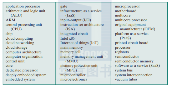
Review Questions
1.1 What, in general terms, is the distinction between computer organization and computer architecture?
1.2 What, in general terms, is the distinction between computer structure and computer function?
1.3 What are the four main functions of a computer?
1.4 List and briefly define the main structural components of a computer.
1.5 List and briefly define the main structural components of a processor.
1.6 What is a stored program computer?
1.7 Explain Moore's law
1.8 List and explain the key characteristics of a computer family. 1.9 What is the kev distinguishing feature of a microprocessor?
Problems
1.1 You are to write an IAS program to compute the results of the following equation.

Assume that the computation does not result in an arithmetic overflow and that X. Y. and N are positive integers with N>=1. Note: lhe IAS did not have assembly language, only machine language
a.Use the equation  when wriling the IAS program.
b.Do it the “hard way"without using the equation from part (a).
1.2 a. On the IAS. what would the machine code instruction look like to load the con- tents of memory address 2 to the accumulator?
- How many trips to memory does the CPU need to make to complete this instruction during the instruction cycle?
1.3 On the IAS. describe in English the process that the CPU must undertake to read a value from memory and to write a value to memory in terms of what is put into the MAR. MBR. address bus.data bus. and control bus.
1.4 Given the memory contents of the IAS computer shown below;

show the assembly language code for the program, starting at address 08A. Explain what this program does.
1.5 In Figure 1.6. indicate the width, in bits, of each data path (e.g. between AC and ALU).
1.6 In the IBM 360 Models 65 and 75. addresses are staggered in two separate main irem- ory units (eg. all even-numbered words in one unit and all odd-numbered words in another). What might be the purpose of this technique?
1.7 The relative performance of the IBM 360 Model 75 is 50 times that of the 360 Model 30, yet the instruction cycle time is only 5 times as fast. How do you account for this discrepancy?
1.8 While browsing at Billy Bobs computer store, you overhear a customer asking Billy Bob what is the fastest computer in the store that he can buy. Billy Bob replies.M You're looking at our Macintoshes, lhe fastest Mac we have runs at a dock speed of 1.2 GHz. If you really want the fastest machine, you should buy our 2.4-GHz Intel Pentium IV instead? Is Billy Bob correct? What would you say to help this customer?
1.9 The ENIAC, a precursor to the ISA machine, was a decimal machine, in which each register was represented by a ring of 10 vacuum tubes. At any time, only one vacaum lube was in the ON state, representing one of the 10 decimal digits. Assuming that ENIAC had the capability to have multiple vacuum tubes in the ON and OFF state simultaneously, why is this representation “wasteful" and what range of integer values could we represent using the 10 vacuum tubes?
1.10 For each of the following examples, determine whether this is an embedded sydem. explaining why or why not.
- Are programs that understand physics and/or hardware embedded? For example, one that uses finite-element methods to predict fluid flow over airplane wings?
- Is the internal microprocessor controlling a disk drive an example of an embedded system?
- I/O drivers control hardware, so does the presence of an I/O driver imply tha: the computer executing the driver is embedded?
- Is a PDA (Ifersonal Digital Assistant) an embedded system?
- Is the microprocessor controlling a cell phone an embedded system?
- Are the computers in a big phased-array radar considered embedded? These radars are 10-story buildings with one to three IOO-foot diameter radiating patches on the sloped sides of the building
- Is a traditional flight management system (FMS) built into an airplane cockpit considered embedded?
- Are the computers in a hardware-in-the-loop (HIL) simulator embedded?
- Is the computer controlling a pacemaker in a persons chest an embedded computer?
- Is the computer controlling fuel injection in an automobile engine embedded?